目次
- 電磁界シミュレーションシリーズ NEC2編 まとめ
- その1アンテナ構造編
- その2プログラム編 給電・負荷・伝送線路・周波数
- その3プログラム編 放射パターン
- その4プログラム編 近傍界
- 応用編 複雑な散乱 CADファイルから物体作成
- 中級編 二つのアンテナ間の伝搬ロスを計算する
- 超入門 4NEC2 と PyNEC
- その他
- よく使うカード
- マニュアルからのカード(コマンド類)の整理
- 旧NEC2 エディタのデータフォーマット
- 4NEC2 エディタのデータフォーマット
- 4NEC2 エディタのヘルプとデータフォーマット
- 定数類
- アンテナ材料の導電率 Wire-conductivity (LD0) for different materials
- 材料の誘電率 Dielectric constant for different materials
- グランド・地面の導電率 Conductivity and diel-constant for differend grounds
- デフォルトの定数 Default SY(mbols)/constants to be used in 4nec2
- 同軸・伝送線路の特性インピーダンスZ0、速度係数Vf Coax/Trans-lines used in stub-matching
- アンテナと伝搬の分かりやすい英語の資料(笑)
- Circuit Design 無線技術情報(こちらは日本語)
- NEC2でどんなことができるか?
- 4NEC2のチュートリアルやブログの記事
- CAEまとめ類
- いいね:
- 関連
電磁界シミュレーションシリーズ NEC2編 まとめ
NEC2を使う場合に、すぐ忘れる NECファイルの意味を4NEC2についているショートリファレンスを元に、忘備録として少し解説を書いておきます。
なお、
言っておくけど。。ここは、むっちゃ簡略版ですよ
その1アンテナ構造編

その2プログラム編 給電・負荷・伝送線路・周波数

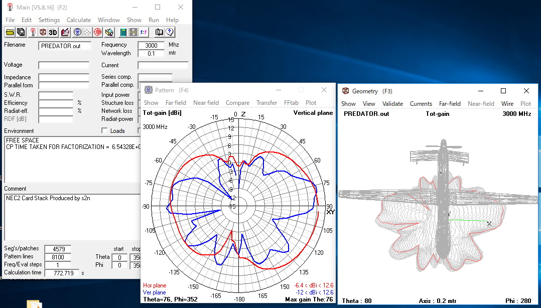
その3プログラム編 放射パターン

その4プログラム編 近傍界

応用編 複雑な散乱 CADファイルから物体作成

中級編 二つのアンテナ間の伝搬ロスを計算する

超入門 4NEC2 と PyNEC

その他
GithubのここにNECファイルなど置いています。

よく使うカード
CM(コメント)
‘ 必要に応じてアポストロフィを使用してコメント行を入力します
CE(コメント終了)
SY(シンボル、その後に使用されるさまざまな因子を定義する変数の宣言、物理量または計算式)
GW(ワイヤーの形状、すべての必要な詳細を含むワイヤーの定義)
GM(生成された構造またはその構造からパーツを回転、移動、またはコピーするために使用されるジオメトリ移動)
GE(ジオメトリの終了、構造入力の終了)。 グランドタイプの追加入力が可能です)
LD(ロード、特定のセグメントのR、L、Cなどの追加コンポーネントを組み込むために使用)
FR(周波数、周波数または掃引範囲の定義)
EK(細いワイヤーの正しいシミュレーションのために追加プログラムを呼び出すために使用される拡張カーネル)
EX(励振、駆動を供給することによる構造の励振)
EN(終わり、終わりのファイル)
マニュアルからのカード(コマンド類)の整理
マニュアル自体はそのまま読めばある程度わかると思いますが、結構間違ったまま記載されていたりするので、いろいろなところを読むのがいいかもしれません。
1.コメントカード(CM、CE)
2.構造形状入力カード
+ワイヤーアーク仕様(GA)
+端部形状入力(GE)
+数値グリーン関数ファイル(GF)
+らせん/らせん仕様(GH)
+座標変換(GM)
+円柱構造(GR)
+スケール構造の寸法(GS)
+ワイヤー仕様(GW)
+座標平面での反射(GX)
+表面パッチ(SP)
+複数のパッチ面 (SM)
3.プログラム制御カード
+最大結合計算(CP)
+拡張細線カーネル(EK)
+終了(EN)
+励起(EX)
+周波数(FR)
+追加の地上パラメーター(GD)
+グランドパラメーター(GN)
+相互作用の近似n範囲(KH)
+負荷・インピーダンス(LD)
+近電界・近磁界(NE、NH)
+ネットワーク(NT)
+構造の接続(NX)
+ワイヤ上の電荷の計算出力(PQ)
+ページタイトル/ワイヤ上の電流の計算出力(PT)
+放射パターン(RP)
+伝送線路(TL)
+ NGFファイルの書き込み(WG)
+実行(XQ)
旧NEC2 エディタのデータフォーマット
! Syntax: <Mnemonic>:<Card_type>:<Column_name>,..,<column_name>
‘ ::4nec2 comment
CE::Comment end, Comment
CM::Comment line, Comment
CP::Maximum coupling calc., tag1, seg1, tag-2, seg2
EK::Extended thin wire kernel
EN::End of input file
EX: :Structure excitation, Type
EX:0:Voltage-source (PEAK values!), Type, Tag, Segm, Option, V (real), V (imag)
EX:1:Incedent wave (linear), Type, Theta, Phi, Option, The ^K, Phi ^K, Eta, incr-The, incr-Phi, Ratio
EX:2:Inced-wave (circ/right), Type, Theta, Phi, Option, The ^K, Phi ^K, Eta, incr-The, incr-Phi, Ratio
EX:3:Inced-wave (circ/left), Type, Theta, Phi, Option, The ^K, Phi ^K, Eta, incr-The, incr-Phi, Ratio
EX:4:I-src (field illumination) , Type, -, -, Option, X (mtr), Y (mtr), Z (mtr), Alpha, Beta, C-moment
EX:5:V-src (current-slope disc), Type, Tag-nr, Seg-nr, Option, V (real), V (imag)
EX:6:Current-source (PEAK values!, 4nec2 specific), Type, Tag, Segm, – , I (real), I (imag)
FR: :Frequency specification, Type
FR:0:Frequency (linear step), Type, Steps, -, -, Start, Stepsize
FR:1:Frequency (logarithmic step), Type, Steps, -, -, Start, Stepsize
GA::Wire arc, Tag, segs, Arc-rad, angle-1, angle-2, wire-rad
GC::Wire radius tapering, -, -, ratio, rad-first, rad-last
GD::Additonal ground specification, -, -, -, -, Diel-const, Conduct, Distance, Height,
GE: :Geometry end, Type
GE:-1:Geometry end (ground plane; current = 0), Type
GE:0:Geometry end (no groundplane), Type
GE:1:Geometry end (ground plane; current expansion), Type
GF: :Read NGF file, Type, [file]
GF:0:Read NGF file (no coords), default, [file]
GF:1:Read NGF file (print coords), coords., [file]
GH::Wire helix/spiral, Tag, segs, spacing, length, rad-X0, rad-Y0, rad-Xl, rad-Yl,Wir-rad
GN: :Ground specification, Type
GN:-1:Free space, Type
GN:0:Finite/Fast gnd, Type, nr-wires, -, -, Diel-const, Conduct, Scr-rad, Wire-rad
GN:1:Perfect ground, Type
GN:2:Real/SomNec gnd, Type, -, -, -, Diel-const, Conduct
GN:3:MiniNec gound (4nec2 specific), Type, -, -, -, Diel-const, Conduct
GM::Coordinate transform, Incr, Nr-str, rotat-X, rotat-Y, rotat-Z, trans-X, trans-Y, trans-Z, start-tag
GR::Cylindrical wire structure, Incr, Nr-str
GS::Scale structure, -, -, Factor
GW::Wire geometry, Tag, segs, X1, Y1, Z1, X2, Y2, Z2, wire-rad
GX::Reflection in coordinate planes, Incr, XYZ
KH::Interaction appr. range, -, -, -, -, distance
LD: :Impedance loading, Type
LD:0:Series RLC, Type, tag-nr, first-S, last-S, Res (ohm), Ind (H), Cap (F)
LD:1:Parallel RLC, Type, tag-nr, first-S, Last-S, Res (ohm), Ind (H), Cap (F)
LD:2:Series impedance, Type, tag-nr, first-S, Last-S, ohm/m, Henry/m, Farad/m
LD:3:Parallel impedance, Type, tag-nr, first-S, Last-S, ohm/m, Henry/m, Farad/m
LD:4:Impedance, Type, tag, first-S, last-S, R(ohm), X(ohm)
LD:5:Wire conductivity, Type, tag-nr, first-S, last-S, G (mho/m)
LD:6:LC-Trap, Type, tag-nr, first-S, last-S, Q-coil, Ind (H), Cap (F), [fr]
LD:7:Wire-coating, Type, tag-nr, first-S, last-S, Diel-const, Radius
NE: :Near electric field, Type
NE:0:Near elec-field (rectang), Type, nr-X, nr-Y, nr-Z, first X, first Y, first Z, X-step, Y-step, Z-step
NE:1:Near elec-field (spheric), Type, nr-R, nr-Phi, nr-The, first R, first Phi, first THe, R-step, The-step, Phi-step
NH: :Near magnetic field, Type
NH:0:Near magn-field (rectang), Type, nr-X, nr-Y, nr-Z, first X, first Y, first Z, X-step, Y-step, Z-step
NH:1:Near magn-field (spheric), Type, nr-R, nr-Phi, nr-The, first R, first Phi, first THe, R-step, The-step, Phi-step
NT::Two port network, tag1, seg1, tag2, seg2, Y11(r), Y11(i), Y12(r), Y12(i), Y22(r), Y22(i)
NX::Next structure
PT: :Print Currents ?, Type
PT:-1:No current, Type
PT:-2:All currents, Type
PT:0:Print current, Type, Tag, first, last
PT:1:Recieving pattern, Type, Tag, first, last
PQ: :Print charges density ?, Type
PQ:-1:No charge densitys, Type
PQ:0:Print charge densitys, Type, Tag, first, last
RP: :Far-field pattern, Type
RP:0:Far-field pattern (default), Type, T-cnt, P-cnt, Option, The-start, Phi-start, The-step, Phi-step, FF-dist, N-gain
RP:1:Far-field and surface wave, Type, Hg-cnt, P-cnt, Option, Hg-start, Phi-start, Hg-step, Phi-step, FF-dist, N-gain
RP:2:Far-field (linear cliff), Type, T-cnt, P-cnt, Option, The-start, Phi-start, The-step, Phi-step, FF-dist, N-gain
RP:3:Far-field (circular cliff), Type, T-cnt, P-cnt, Option, The-start, Phi-start, The-step, Phi-step, FF-dist, N-gain
RP:4:Far-field (ground screen), Type, T-cnt, P-cnt, Option, The-start, Phi-sta, The-step, Phi-step, FF-dist, N-gain
RP:5:Far-field (screen+linear-cliff), Type, T-cnt, P-cnt, Option, The-start, Phi-start, The-step, Phi-step, FF-dist, N-gain
RP:6:Far-field (screen+circular-cliff), Type, T-cnt, P-cnt, Option, The-start, Phi-start, The-step, Phi-step, FF-dist, N-gain
SC::Surface patch continuation, -, Shape, X3, Y3, Z3, (X4), (Y4), (Z4)
SM::Multiple surface patch, nr-X, nr-Y, X1, Y1, Z1, X2, Y2, Z2
SP::Surface patch, -, Shape, X1/cent-X, Y1/cent-Y, Z1/cent-Z, X2/elev, Y2/azim, Z2/area
SY::4nec2 Symbol definition, Symbols
TL::Transmission line, tag1, seg1, tag2, seg2, char-imp, length, G1, Y1, G2, Y2
WG::Write NGF file, [file]
XQ:*:Execute input file
4NEC2 エディタのデータフォーマット
! Syntax: <Mnemonic>:<Card_type>:<Column_name>,..,<column_name>
‘ ::4nec2 comment
CE::Comment end, Comment
CM::Comment line, Comment
CP::Maximum coupling calc., tag1, seg1, tag2, seg2
CW::Catenary wire, Tag, segs, X1, Y1, Z1, X2, Y2, Z2, wire-rad, type, dist, (dZ)
EN::End of input file
EX: :Structure excitation, Type
EX:0:Voltage-source (PEAK values!), Type, tag, segm, option, V (real), V (imag), norm-fact
EX:1:Plane wave (linear), Type, Theta, Phi, option, The ^K, Phi ^K, Eta, incr-The, incr-Phi, ratio, E-fld
EX:2:Plane wave (circ/right), Type, theta, phi, option, the ^K, phi ^K, eta, incr-The, incr-Phi, ratio. E-fld
EX:3:Plane wave (circ/left), Type, theta, phi, option, the ^K, phi ^K, eta, incr-The, incr-Phi, ratio, E-fld
EX:4:I-src (field illumination) , Type, -, -, option, X (mtr), Y (mtr), Z (mtr), alpha, beta, C-moment
EX:5:V-src (bicone source), Type, tag-nr, seg-nr, Option, V (real), V (imag), norm-fact
EX:6:Current-source (PEAK values!, 4nec2 specific), Type, tag-nr, seg-nr, – , I (real), I (imag), norm-fact
FR: :Frequency specification, Type
FR:0:Frequency (linear step), Type, steps, -, -, start, step
FR:1:Frequency (logarithmic step), Type, Steps, -, -, start, step
GA::Wire arc, Tag, segs, arc-rad, angle-1, angle-2, W-rad
GC::Tapered wire, flag, -, ratio, rad-first, rad-last, len-first, len-last
GD: :Additonal ground specification, Type
GD:1:Ground (linear boundary), Type, diel-C, donduct, dist-X, height
GD:2:Ground (circular boundary), Type, diel-C, donduct, distance, height
GE: :Geometry end, Type, check
GE:-1:Geometry end (ground plane; current = 0), Type, check
GE:0:Geometry end (no groundplane), Type, check
GE:1:Geometry end (ground plane; current expansion), Type, check
GF: :Read NGF file, Type, [file]
GF:0:Read NGF file (no coords), default, [file]
GF:1:Read NGF file (with end coords), coords., [file]
GH::Wire helix/spiral, Tag, turns, len-Z, rad-start, rad-end, Wrad-start, Wrad-end, type
GN: :Ground specification, Type
GN:-1:Free space, Type
GN:0:Finite/Fast gnd, Type, Nr-wires, -, -, Diel-C, Conduct, rad-scr, rad-wire
GN:1:Perfect ground, Type
GN:2:Real/SomNec gnd, Type, -, -, -, Diel-C, Conduct, Diel-2, Cond-2, Dist-X, Height, (file)
GN:3:MiniNec ground (4nec2 specific), Type, -, -, -, Diel-C, Conduct
GM::Coordinate transform, Incr, Nr-str, rot-X, rot-Y, rot-Z, move-X, move-Y, move-Z, tag1, seg1, tag2, seg2
GR::Cylindrical wire structure, Incr, Nr-str
GS::Scale structure, -, -, Factor
GW::Wire geometry, Tag, segs, X1, Y1, Z1, X2, Y2, Z2, wire-rad
GX::Reflection in coordinate planes, Incr, XYZ
IS: :Insulated wire, Option
IS:0:Insulated wire (Set), Option, tag-nr, first-S, last-S, diel-C, conduct., radius
IS:-1:Insulated wire (Clear), Option, tag-nr, first-S, last-S, diel-C, conduct., radius
JN: :Junction charge distrib, Option
JN:0:Charge distrib -> Log(ka), Option
JN:-1:Charge distrib -> MOM, Option
LD: :Impedance loading, Type
LD:0:Series RLC, Type, tag-nr, first-S, last-S, Res (ohm), Ind (H), Cap (F)
LD:1:Parallel RLC, Type, tag-nr, first-S, Last-S, Res (ohm), Ind (H), Cap (F)
LD:2:Series impedance, Type, tag-nr, first-S, Last-S, ohm/m, Henry/m, Farad/m
LD:3:Parallel impedance, Type, tag-nr, first-S, Last-S, ohm/m, Henry/m, Farad/m
LD:4:Impedance, Type, tag, first-S, last-S, R(ohm), X(ohm)
LD:5:Wire conductivity, Type, tag-nr, first-S, last-S, G (mho/m), permeab.
LD:6:LC-Trap, Type, tag-nr, first-S, last-S, Q-coil, Ind (H), Cap (F), [fr]
LD:7:Wire-coating, Type, tag-nr, first-S, last-S, Diel-const, Radius
LE: :E-field along line, Option
LE:0:E-fld along line (default, Option, nr-pts, X1, Y1, Z1, X2, Y2, Z2
LE:-1:E-fld along line (reset Integral), Option, nr-pts, X1, Y1, Z1, X2, Y2, Z2
LH: :H-field along line, Option
LH:0:H-fld along line (default, Option, nr-pts, X1, Y1, Z1, X2, Y2, Z2
LH:-1:H-fld along line (reset Integral), Option, nr-pts, X1, Y1, Z1, X2, Y2, Z2
NE: :Near electric field, Type
NE:0:Near elec-field (rectang), Type, nr-X, nr-Y, nr-Z, first X, first Y, first Z, X-step, Y-step, Z-step
NE:1:Near elec-field (spheric), Type, nr-R, nr-Phi, nr-The, first R, first Phi, first THe, R-step, The-step, Phi-step
NH: :Near magnetic field, Type
NH:0:Near magn-field (rectang), Type, nr-X, nr-Y, nr-Z, first X, first Y, first Z, X-step, Y-step, Z-step
NH:1:Near magn-field (spheric), Type, nr-R, nr-Phi, nr-The, first R, first Phi, first THe, R-step, The-step, Phi-step
NT::Two port network, tag1, seg1, tag2, seg2, Y11 (r), Y11 (i), Y12 (r), Y12 (i), Y22(r), Y22(i)
NX::Next structure
PT: :Print Currents, Type
PT:-2:All currents, Type
PT:-1:No currents, Type
PT:0:Print segment current, Type, Tag, first, last
PT:1:Recieving pattern, Type, Tag, first, last
PT:2:Recieving pattern normalized, Type, Tag, first, last
PT:3:Recieving pattern one segment, Type, Tag, first, last
PQ: :Print charge densitys, Type
PQ:-1:No charge densitys, Type
PQ:0:Print charge densitys, Type, Tag, first, last
PS::Print electical lengths
RP: :Far-field pattern, Type
RP:0:Far-field pattern (default), Type, The-cnt, Phi-cnt, XNDA, The-start, Phi-start, The-step, Phi-step, R-dist, G-norm
RP:1:Far-field plus surf-wave, Type, Hg-cnt, Phi-cnt, XNDA, Hg-start, Phi-start, Hg-step, Phi-step, R-dist, G-norm
SC::Surface patch continuation, -, Shape, X3, Y3, Z3, (X4), (Y4), (Z4)
SM::Multiple surface patch, nr-X, nr-Y, X1, Y1, Z1, X2, Y2, Z2
SP::Surface patch, -, Shape, X1/cent-X, Y1/cent-Y, Z1/cent-Z, X2/elev, Y2/azim, Z2/area
SY::4nec2 Symbol definition, Symbols
TL::Transmission line, tag1, seg1, tag2, seg2, char-imp, length, G1, Y1, G2, Y2
UM::Upper medium params, -, -, -, -, diel-C, conduc.
VC: :V-source end caps, option
VC:0:V-source end caps (set), option
VC:-1:V-source end caps (reset), option
WG::Write NGF file, [file]
XQ:*:Execute input file
4NEC2 エディタのヘルプとデータフォーマット
! Syntax: <NEC_card>, <grid_col_nr(s)> = <help_text>
SY,1=Symbol/Variable with value or equation
SY,2=Optional comment on symbol/variable
GW,1=Default straight line wire-element
GW,2=Zero (0) or Tag-number assigned to all segments of the wire (>9800 dont show, >9900 4nec2 specific)
GW,3=Number of segments into which the wire will be divided
GW,4=End-1: X coordinate
GW,5=End-1: Y coordinate
GW,6=End-1: Z coordinate
GW,7=End-2: X coordinate
GW,8=End-2: Y coordinate
GW,9=End-2: Z coordinate
GW,10=Wire/element radius (diameter/2) & Ratio of length of a segment to the length of previous segment
GW,11=Wire radius (diameter/2) for first segment
GW,12=Wire radius (diameter/2} for last segment
GH,1=Helical shaped wire-element
GH,2=Zero (0) or tagnumber to identify helix
GH,3=Number of segments for the helix
GH,4=Spacing between turns
GH,5=Total length of Helix
GH,6=Radius in X at end-1
GH,7=Radius in Y at end-1
GH,8=Radius in X at end-2
GH,9=Radius in Y at end-2
GH,10=Wire radius (diameter/2)
GA,1=Arc shaped wire-element
GA,2=Zero (0) or Tag-nr assigned to all segments of the wire arc
GA,3=Number of segments into which the arc will be divided
GA,4=Arc radius (center is the origin and the axis is the y-axis)
GA,5=Angle of first end of the arc measured from the x axis in a left-hand direction about the y axis (degrees).
GA,6=Angle of the second end of the arc.
GA,7=Wire radius (diameter/2)
GM,1=Move and/or rotate above wires and/or surface patches
GM,2=Tag number increment for moved/copied structures
GM,3=Number of new structures to be generated (0 for move only)
GM,4=Angle in degrees through which the structure is rotated about the X-axis
GM,5=Angle of rotation about the Y-axis
GM,6=Angle of rotation about the Z-axis
GM,7=X direction by which the structure is moved
GM,8=Y direction by which the structure is moved
GM,9=Z direction by which the structure is moved
GM,10=Tag-number to specify start of wire-set to move/copy
GM,11=Tag-number to specify end of wire-set to move/copy
GX,1=Mirror above wires and/or surface-patches in X, Y and/or Z-plane
GX,2=Tag number increment for reflected structures
GX,3=Mirror in YZ plane (along X-axis)
GX,4=Mirror in XZ plane (along Y-axis)
GX,5=Mirror in XY plane (along Z-axis)
GR,1=Rotate above wires and/or surface-patches around Z-axis
GR,2=Tag number increment for each new structure
GR,3=Total number of times that the structure is to occur around the Z-axis
GS,1=Select desired scaling factor for Geometry data
GS,2=User specified geometry scaling factor
LD01234567,2=Tag-nr of wire to place load(s) (0 for whole structure)
LD01234567,3=First wire-segment to place load(s) (0 for whole wire)
LD01234567,4=Last wire-segment to place load(s) (0 for whole wire)
LDO,1=Series RLC load
LD1,1=Parallel RLC load
LD01,5=Resistance for spot-load in Ohms
LD01,6=Inductance for spot-load in Henrys
LD01,7=Capacitance for spot-load in Farads
LD2,1=Distributed series RLC load
LD3,1=Distributed parallel RLC load
LD23,5=Distributed resistance in ohms per meter
LD23,6=Distributed inductance in Henrys per meter
LD23,7=Distributed capacitance in Farads per meter
LD4,1=R+jX impedance
LD4,5=Resistance in Ohms
LD4,6=Reactance in Ohms (+/-)
LD5,1=Wire conductivity
LD5,5=Select wire material or enter conductivity in Siemens
LD6,1=LC trap
LD6,5=Q(uality)-factor of coil
LD6,6=Inductance of coil in Henrys
LD6,7=Value of parallel capacitor in Farads
LD6,8=Optional trap design frequency
LD7,1=Insulated wire
LD7,5=Select insulating material or enter dielectric-constant
LD7,6=Radius of insulating material (diameter/2)
EX0,1=Standard Voltage source (Peak value)
EX1,1=incident plane wave, linear polarization
EX2,1=incident plane wave, right-hand polarization
EX3,1=incident plane wave, left-hand polarization
EX4,1=Elementary current source
EX5,1=Voltage-src (current-slope-discontinuity).
EX6,1=Standard Current source (Peak value)
EX056,2=Tag-number of wire to place the source
EX056,3=Segment-number on wire to place the source
EX123,2=Nr of theta angles desired for the incident plane-wave
EX123,3=Nr of phi angles desired for the incident plane-wave
EX4,2=No data, use “0”
EX4,3=No data, use “0”
EX0123456,4=Optional reporting options. See Nec-manual
EX056,5=Real part of peak-voltage/current in Volts/Amperes.
EX056,6=Imaginary part of peak-voltage/current in Volts/Amperes.
EX056,7=Magnitude of peak-voltage/current in Volts/Amperes.
EX056,8=Phase angle in degrees of voltage/current.
EX056,9=Optional normalization value, see Nec-manual
EX123,5=Theta spherical coordinate, measured from the Z-axis
EX123,6=Phi spherical angle in XY, measured around Z-axis
EX123,7=Eta polarization angle (linear polarization) or major elllipse axis
EX123,8=Theta angle stepping increment
EX123,9=Phi angle stepping increment
EX123,10=Ratio of minor to major axis for elliptic-polarization
EX4,5=X position in @m.
EX4,6=Y position in @m.
EX4,7=Z position in @m.
EX4,8=Alpha angle in degrees the current source makes with the XY plane
EX4,9=Beta angle the projected current on XY makes with the Y-axis
EX4,10=”Current moment” of the source in Amp-meters.
TL,1=Transmission-line between any two segments on structure
TL,2=Tag-nr for the wire to wich end-1 of the line is connected
TL,3=Segment-nr on the wire to which end-1 of the line is connected
TL,4=Tag-nr for wire at end-2 of the line
TL,5=Segment-nr on wire at end-2 of the line
TL,6=Char-impedance in ohms (negative indicates twisted line)
TL,7=Electrical line-length in @m. If zero, straight line distance is used
TL,8=Select open/short end or enter real part of shunt admittance at end-1
TL,9=Optional: imaginary part of the shunt admittance at end-1
TL,10=Select open/short end or enter real part of shunt admittance at end-2
TL,11=Optional: imaginary part of the shunt admittance at end-2
NT,1=Two port none-radiating network
NT,2=Tag-nr for the wire to wich port-1 of network is connected
NT,3=Segment-nr on the wire to which port-1 is connected
NT,4=Tag-nr for wire at port-2
NT,5=Segment-nr on wire at port-2
NT,6=Real part of element [1, 1] in mhos
NT,7=Imaginary part of element [1, 1] in mhos
NT,8=Real part of element [1, 2]
NT,9=Imaginary part of element [1, 2]
NT,10=Real part of element [2, 2]
NT,11=Imaginary part of element [2, 2]
SP0,1=Arbitrary shaped surface patch
SP1,1=Rectangular surface patch
SP2,1=Triangular surface patch
SP3,1=Quadrilateral surface patch
SP0,2=X coordinate of patch center
SP0,3=Y coordinate of patch center
SP0,4=Z coordinate of patch center
SP0,5=elevation angle above the XY plane of outward normal vector (degrees)
SP0,6=azimuth angle from X-axis of outward normal vector (degrees)
SP0,7=patch area (square of units used)
SP123,2=Corner 1: X coordinate
SP123,3=Corner 1: Y coordinate
SP123,4=Corner 1: Z coordinate
SP123,5=Corner 2: X
SP123,6=Corner 2: Y
SP123,7=Corner 2: Z
SP123,8=Corner 3: X
SP123,9=Corner 3: Y
SP123,10=Corner 3: Z
SP3,11=Corner 4: X
SP3,12=Corner 4: Y
SP3,13=Corner 4: Z
SC,1=Rectangular or Quadrilateral surface patch continuation
SC,2=Next patch, corner 3: X (corner 1 is corner 3 previous patch)
SC,3=Next patch, corner 3: Y
SC,4=Next patch, corner 3: Z
SC,5=Next patch, corner 4: X (corner 2 is corner 4 previous patch)
SC,6=Next patch, corner 4: Y
SC,7=Next patch, corner 4: Z
SM,1=Multiple (rectangular) surface patch
SM,2=Number of patches from corner 1 to 2
SM,3=Number of patches from corner 2 to 3
FR,1=Check to run frequency sweep
FR,2=Number of calculation steps in sweep
FR,5=(Start) Frequency in Mhz
FR,6=Frequency increment in Mhz
GN,1=Select antenna environment / ground approximation
GN,2=Number of radial wires in ground-plane
GN,3=Check to include radial ground-screen
GN,4=Select type of ground to use
GN,5=Ground conductivity in Siemens
GN,6=Dielectric constant of ground
GN,7=Length of radial wires in @m.
GN,8=Radius of the wires used in the screen, in mm
GD,1=Check to include secondary/distant ground
GD,7=Distance from the origin in @m.
GD,8=Depth below main ground in @m.
EK,1=Check to use Extended Kernel (for fat wires)
GF,1=Check to read geometry from specified file
GF,2=Name of file to write/read geometry from/to
WG,1=Check to write geometry to specified file
定数類
アンテナ材料の導電率 Wire-conductivity (LD0) for different materials
! Format: <Name> = <value>
例
LD5,1=Wire conductivity
LD5,5=Select wire material or enter conductivity in Siemens
LD 5 1 0 0 58000000 ’Copper
Perfect = 9.9E+99
Silver = 62900000
Copper = 58000000
Alumin. = 37700000
Alu-T832 = 30800000
Alu-T6 = 24900000
Brass = 15600000
P-bronze = 9090000
St-Steel = 1390000
Insulator= 0.00001
Carbon-fiber = electrical conductivity (106 S/m)

材料の誘電率 Dielectric constant for different materials
! Syntax: <Name> = <value>
Al-oxide = 10
Cu-oxide = 18
Nylon = 3.4
Paper = 2.2
Pertinax = 4.9
Plexiglas = 3.1
Polycarb. = 3.2
Polyethyl. = 2.4
Polystyr. = 2.7
PVC (hard) = 3.5
PVC (soft) = 4.5
Rubber = 2.9
Shellac = 3.3
Styrofoam = 1.03
Teflon = 2.1
Wind-glas = 7.6
Wood (dry) = 2.3
グランド・地面の導電率 Conductivity and diel-constant for differend grounds
! Format: <Name> = <conductivity>,<dielectric_constant>
! http://pe2bz.philpem.me.uk/Comm/-%20Antenna/Info-905-Misc/soildiel.htm
Poor = 0.001, 5
Moderate = 0.003, 4
Average = 0.005, 13
Good = 0.015, 17
Dry, sandy, coastal = 0.001, 10
Pastoral hills, rich soil = 0.007, 17
Medium hills and forest = 0.004, 13
Mountainous hills < 1000m = 0.002, 5
Rocky, steep hills = 0.002, 13
Fertile land = 0.002, 10
Rich agric. land, low hills = 0.01, 15
Marshy land, densily wooded = 0.0075, 12
Marshy, forested, flat = 0.008, 12
Highly moist ground = 0.005, 30
City industrial area = 0.0001, 3
City industr. average att. = 0.001, 5
City industr. maximum att. = 0.0004, 3
Fresh water = 0.001, 80
Fresh water 10ー/100 Mhz = 0.001, 84
Fresh water 20ー/100 Mhz = 0.005, 80
Sea water = 5.0, 81
Sea water 10ー, up to 1 Ghz = 4.0, 80
Sea water 20ー, up to 1 Ghz = 4.0, 73
Sea ice = 0.001, 4
Polar ice = 0.0003, 3
Polar ice cap = 0.0001, 1
Artic land = 0.0005, 3
<user specified> = ,
デフォルトの定数 Default SY(mbols)/constants to be used in 4nec2
Pi=3.14159265358979
! AWG wire radi in mm’s
#0=8.2525mm/2
#1=7.3482mm/2
#2=6.5430mm/2
#3=5.8268mm/2
#4=5.1892mm/2
#5=4.6203mm/2
#6=4.1148mm/2
#7=3.6652mm/2
#8=3.2639mm/2
#9=2.9058mm/2
#10=2.5883mm/2
#11=2.3038mm/2
#12=2.0523mm/2
#13=1.8288mm/2
#14=1.6281mm/2
#15=1.4503mm/2
#16=1.2903mm/2
#17=1.1506mm/2
#18=1.0236mm/2
#19=0.9119mm/2
#20=0.8128mm/2
同軸・伝送線路の特性インピーダンスZ0、速度係数Vf Coax/Trans-lines used in stub-matching
! Syntax: <name> – <Z0>, <Vf>
RG6 – 75, 0.75
RG8 – 52, 0.66
RG8A – 52, 0.66
RG8X – 50, 0.78
RG8 foam – 50, 0.78
RG11 – 75, 0.66
RG11A – 75, 0.66
RG11 foam – 75, 0.78
RG58 – 53.5, 0.66
RG58A – 50, 0.66
RG58C – 50, 0.66
RG58A foam – 53.5, 0.78
RG59 – 75, 0.66
RG59 foam – 75, 0.79
RG213 – 50, 0.86
Twin 75 ohm – 75, 0.67
Twin flat – 300, 0.82
Twin tube – 300, 0.80
Open line A – 300, 0.95
Open line B – 450, 0.95
アンテナと伝搬の分かりやすい英語の資料(笑)
Electromagnetic Waves and Antennas

無線用語集
設計ガイド
ARIB標準規格
NEC2でどんなことができるか?
は、このページなどがいいかと思います。
How to Start Modeling Antennas using EZNEC
Olde Skool Antenna Design with NEC2 on OpenBSD
Part I:NEC Program Description – Theory
Part III:NEC User’s Guide
4NEC2のチュートリアルやブログの記事
- インストール方法
- 4NEC2で4エレ円形アンテナの解析などされています。
- 4NEC2でSRA(スーパーラドアンテナ)をシミュレート1
- いろいろなアンテナ解析
- いろいろなアンテナ解析
- 3DビームやF/B比の表示方法
- 4NEC2 Definitive Guide
- EzNECを用いたシミュレーション法など線状アンテナいっぱい(ON5NAU)
これおすすめ
上級編
CAEまとめ類

コメントを残していただけるとありがたいです